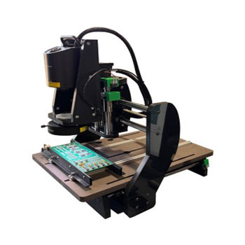
NovaScope SS-XYZ-T
 The NovaScope SS-XYZ-T is a Photo-Documentation and Optical Inspection System for printed circuit board assemblies. It combines a Targano ZAP digital microscope and Ring Light with a computer controlled XY & Z positioner to automatically move the scope to visual inspection locations or automatic image capture locations on the circuit board. The circuit board can also be left in place while performing certain rework operations.
The NovaScope can significantly increase the speed and accuracy of human visual inspections. Programming can be done quickly using the XY Placement List and Bill of Material import features. There is also a utility for simple matrix type inspection or photo-documentation and image stitching of the board.
In comparator mode the system shows a live image from the microscope next to a reference image for visual comparison by the operator. Images are automatically captured and saved as part of a post-inspection report. As an option, the system can also be configured with some AOI.
The NovaScope is a powerful inspection and documentation tool for:
- High Reliability applications (MIL-Spec, Medical, Automotive)
- Hi-Mix Low-Volume operations
- First Article Inspection
- Solder Joints and Tall Thru-hole Parts
- Conformal Coating
- Assembly Line Auditing
- Cleanliness/FOD/Tin Whisker detection
Ideal for Inspecting: Part Presence, Rotation, Polarity, Registration, Text, Solder, Solder Paste, Bent Leads, Bent Pins, Jumpers, Cut Traces, or any other top-down visual feature on the PCBA.
System Specifications (subject to change)
Base Model |
NovaScope SS-XYZ-T |
Standard Digital Microscope |
TAGARNO FHD ZAP w/ +4 lens Full HD Image (1920x1080) 30x Optical Zoom Mag. 1.7x - 52.7x, FOV 11.42” - 0.43”, WD 9.84” |
Optional Digital Microscopes |
DeltaPix, Unitron, and other USB Microscopes and Cameras |
Optional Lighting |
TAGARNO Ring Lamp (white or UV), coaxial light, back light |
Top Clearance |
3” Top Side Clearance above PCB |
Bottom Clearance |
1” Bottom Side Clearance below PCB |
Inspection Area |
12” x 13” and 4” Z |
Dimensions |
15” wide x 21” long x 22” high |

